Semiconductor Fabrication: A Complete Guide to Chip Manufacturing Processes
Semiconductor fabrication is the process used to create tiny electronic components called integrated circuits, commonly known as chips. These chips are the foundation of modern technology and are used in devices such as smartphones, computers, automobiles, and medical equipment.
Fabrication of semiconductors matters since it reveals how modern devices come together. With tech moving forward, needing chips that run quicker, take less space, becomes stronger - so this method gains ground. Though unseen by most, its role grows alongside digital progress.
semiconductor fabrication process explained
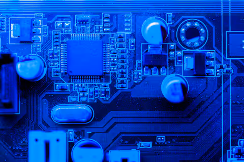
Out in clean rooms where air stays filtered, tiny circuits get built step by step onto smooth wafers - most often crafted from silicon. These spots? Called fabs, they’re set up just for crafting chips without dust or dirt messing things up
Key Characteristics
- Uses ultra-pure materials
- Requires cleanroom environments
- Involves nanoscale precision
- Fully automatic, yet carefully managed
Common Material Used
Tiny bits of sand help make chips work. This glassy stuff keeps parts from touching. Wires made of shiny elements carry power. A special film shifts designs onto surfaces. Each piece has a job in building tiny circuits.
Why Making Computer Chips Matters
Fine grains of silicon become tiny brains inside machines when shaped by precise tools. Because these pieces guide electricity, they make phones talk and computers think. Machines build them layer after layer, each one thinner than dust. Without such careful crafting, daily tech would simply stop breathing.
Why It Matters
- Backs progress in tech by making room for smarter gadgets to grow
- Built for speed, these chips handle tasks quicker. Efficiency climbs because design cuts delays. Power use drops without slowing down. Faster response comes from smarter layout. Output jumps when circuits work smoother
- Miniaturization: Helps reduce device size while increasing capability
- Worldwide progress powers fields like artificial intelligence, cars, when it comes to medical care
Fabrication Types and Main Features
Building chips relies on a range of key methods used during semiconductor manufacturing. What shapes the process comes down to specific tools and steps applied carefully at each stage.
Welding Casting Molding Forging
1. Front-End Processing
This process builds transistors directly onto the silicon surface. Components form through precise layering steps across the wafer. Tiny circuits take shape using light and chemical treatments. Each feature emerges gradually during fabrication stages. Structures grow one level at a time under controlled conditions.
2. Back-End Processing
Wiring things together happens through thin sheets of metal, setting up what comes next. The chip gets ready as these links take shape across its surface.
Key Aspects
- Photolithography: Transfers circuit patterns onto the wafer
- Etching: Removes unwanted material to create structures
- Doping: Adds impurities to control electrical properties
- Deposition: Adds thin layers of materials
Inside Chip Making Plants
Starting with raw materials, each stage unfolds slowly through repetition, forming thin layers one after another. Though it seems messy at first, movement between phases creates order gradually instead of all at once.
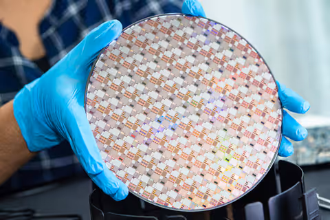
1. Wafer Preparation
- Fine grains of silicon get cleaned through a careful process. These pure pieces are then formed into flat discs. Thin slices come next, cut with precision tools
- Surface is polished to achieve smoothness
2. Oxidation
- Fine coating of oxygen builds up across the chip's face. This skin appears after exposure to air. Surface changes happen slowly. Material reacts when left out. A film shows on top. Reaction takes place at room conditions. Layer grows thinner than a hair. Outside touch alters the base
- Acts as an insulating barrier
3. Photolithography
- A thin layer that reacts to light gets put on. This coating, called photoresist, goes down first. It waits for exposure next
- Patterns reach the wafer by ultraviolet light
4. Etching
- Unwanted material is removed
- Creates precise circuit patterns
5. Doping
- Some chemical contaminants get included
- Controls conductivity of the semiconductor
6. Deposition
- Thin layers of materials are added
- Builds multiple layers of circuits
7. Metallization
- Metal layers are added for electrical connections
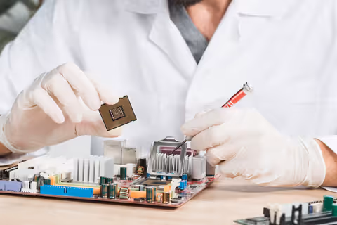
8. Testing and Packaging
- Chips are tested for functionality
- Wrapped up tight, ready to slide inside gadgets without a hitch
Recent Shifts in Chip Manufacturing
Faster chips now emerge as fresh methods boost how well they work. Progress surges when clever designs reshape what circuits can do.
Recent Developments
- Smaller Node Sizes: Chips are now built at 3nm and below
- Extreme Ultraviolet (EUV) Lithography: Enables finer patterning
- 3D Chip Stacking: Improves performance and space usage
- Advanced Materials: Use of new compounds beyond silicon
- Robots working alongside smart software make tasks more accurate. Accuracy improves when machines learn from patterns instead of fixed rules. Mistakes fade as systems adjust on their own. Learning happens step by step through repeated actions. Precision grows without constant human oversight
common mistakes and things to consider
Fabrication of semiconductors demands exactness; tiny flaws might alter how well they work.
Common Challenges
- Fine grains settle where they should not, wrecking delicate pathways inside machines
- Temperature Control: Variations can affect material properties
- Complex Process Management: Requires strict sequencing
- High Precision Requirements: Nanometer-scale accuracy is essential
Key Considerations
- Maintain cleanroom standards
- Line things up just right when doing lithography
- Monitor material quality
- Use advanced testing methods
Conclusion
Out of silicon wafers come tiny circuits built layer by layer through careful shaping and etching. Starting clean, the material moves through stages where light, heat, and gases reshape it bit by bit. One slip in temperature or timing throws everything off balance. Hidden patterns form under microscopes, invisible yet vital to how phones and computers run. After testing, each chip gets sealed safely inside protective shells. Precision drives every move, no room for guesswork.
When tech moves forward, making semiconductors stays central to change, backing improvements in computers, messaging systems, while shaping machines that work on their own. Grasping how it happens reveals what goes into the gadgets people use every day.