Semiconductor Design Process: A Complete Guide to Modern Chip Development
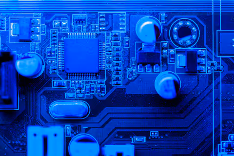
The semiconductor design process is the method used to create integrated circuits (ICs), which are the foundation of modern electronics. From smartphones and laptops to cars and smart devices, semiconductors power almost everything around us.
Most folks overlook how gadgets come together, yet it reveals why today’s electronics work so smoothly. When tech moves forward, chips adapt too - suddenly everything runs quicker, fits tighter, uses less power.
This guide breaks down how chips are made using everyday words, so anyone can follow along without prior knowledge. Starting with basic ideas, it walks through each step clearly. Because clarity matters, complex jargon gets swapped for familiar language. Readers learn by example rather than theory, building understanding slowly. Through steady pacing, even tough parts feel manageable. With no assumed background, newcomers find their footing fast. Each idea connects to the next like steps on a path forward.
How Chips Are Made From Idea To Production
A single thought kicks off what becomes a working chip, step by step. Through layers of planning, the concept takes shape slowly. Engineering meets code, guided by precision tools along the way. Production methods enter early, shaping how everything fits together. Each phase links tightly, one after another, building toward something real.
Key Stages Overview
What happens first? Requirements get defined along with how things should work. Next up, the chip's framework takes shape through planning and logical setup. After that, checks happen to confirm whether everything works correctly. Then comes turning those plans into actual floorplans on silicon. Once designed, real production begins - chips are built piece by piece. Lastly, each unit is checked again then packed ready for its role.
Without one step, the last piece might fail when it counts. How a tiny part behaves now shapes what happens later. Every shift along the way holds weight in how fast it runs. Missing any moment could break the rhythm needed at the end.
Semiconductor Design Matters
A single chip begins long before machines power on. Design shapes how devices think today. Ideas form circuits that hum inside smart tools everywhere. Creation happens step by step, quiet and precise. Every pathway carved in silicon starts with intent.
Why It Matters
- Enables development of advanced electronics
- Improves device performance and efficiency
- Healthcare moves forward because of fresh ideas. In cars, new thinking shapes how things work. Talking to each other gets easier when systems improve. Each field grows a little differently. Progress shows up where people try something else
- Using less energy means cooler operation. Power draw drops when efficiency rises. Less waste shows up as lower temps. Efficiency gains cut down on excess warmth. Cooler systems often need simpler cooling
- Allows miniaturization of electronic components
A chip might stop working if its layout is off. Poor planning can make it drain energy fast. Its speed could lag when details are ignored.
semiconductor design essentials
What shapes chip creation? Key pieces play a role. Each part matters more than it first seems. How things fit together drives the whole process. Pieces interact in ways not always obvious at first glance.
1. Design Specifications
This begins when engineers lay out what needs doing
- Functionality of the chip
- Performance requirements
- Power and size constraints
2. languages for describing hardware
Folks write chip designs using code, often picking something like Verilog. Code shaped this way turns into actual circuits later on. Instead of drawing parts by hand, engineers sketch them with words in languages such as VHDL. What looks like software at first becomes hardware when built. These tools let logic take shape before any physical piece exists.
3. Tools for designing electronic systems
Simulation, verification, layout creation - these jobs get handled faster when EDA tools step in. Tasks that once took ages now move smoothly, thanks to automated support behind the scenes.
4. Logic Design
Logic gates help engineers build digital circuits that do specific jobs. Circuits come alive when signals flow through tiny electronic switches working together. These setups follow strict rules so everything runs smoothly every time. Digital systems rely on precise arrangements of these components to handle tasks correctly.
5. Physical Constraints
Design must consider:
- Chip size
- Power consumption
- Heat dissipation
How Chips Are Made From Start to Finish
A step-by-step path guides how chips are designed. From start to finish, each phase builds on what came before it.
1. Specification and Planning
What comes first is deciding the job of the chip. That step covers:
- Performance targets
- Functional requirements
- Power limits
2. System Architecture Design
A blueprint takes shape on paper first. Outlines appear showing where parts go. Some sections link together early. Others wait till later steps. Designers sketch big blocks before tiny details. Lines form around power areas next. Ideas shift slightly during reviews. Decisions lock once testing begins
- Block diagrams
- Data flow design
- Component interaction
3. rtl design register transfer level
At this stage:
- Logic is written using HDL
- Data flow between registers is defined
4. Functional Verification
Verification ensures the design works as intended:
- Simulation tools test different scenarios
- Fixes show up fast because problems get spotted right away
5. Synthesis
The HDL code is converted into a gate-level representation:
- Logical circuits are mapped to real hardware elements
6. Physical Design
Out here, thoughts take shape as actual design. Where ideas meet space, structure appears. Not just concepts anymore - lines form on the page. Through this step, thinking gets built, one piece at a time. Shape rises where meaning was only planned
- Placement of components
- Routing of connections
7. Timing and Power Analysis
Engineers analyze:
- Signal delays
- Power usage
- Performance optimization
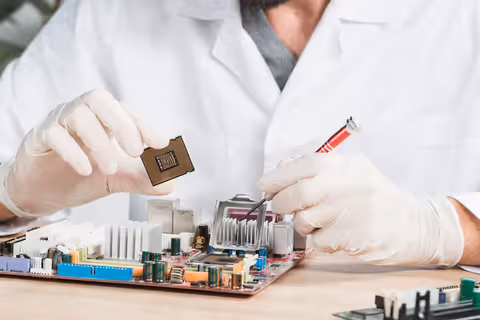
8. Fabrication (Manufacturing)
Fabrication shops receive the blueprint next. Workers there begin building once plans arrive. Each part gets made following exact sketches. Machines cut materials after engineers approve layouts. Production moves forward when everything aligns properly
- Silicon wafers are processed
- Transistors are created
9. Testing and Packaging
After manufacturing:
- Chips are tested for defects
- Wrapped up tight, ready to slide inside gadgets without a hitch
Future Directions in Chip Development 2025 to 2026
Faster changes now shape how chips get made. New ideas pop up almost every month.
1. AI-Assisted Design
Artificial intelligence is being used to:
- Optimize chip layouts
- Reduce design time
- Improve efficiency
2. Advanced Node Technology
Smaller process nodes (like 3nm and below) allow:
- Higher performance
- Lower power consumption
3. Chiplet Architecture
Instead of one large chip:
- Multiple smaller chips are combined
- Improves flexibility and scalability
4. 3D IC Design
Stacking chips vertically:
- Saves space
- Enhances performance
5. Energy Efficiency First
Modern designs prioritize:
- Low power consumption
- Sustainable computing
common mistakes and things to consider
Working on chip designs brings challenges; some problems might change results.
Common Mistakes
- Incomplete design specifications
- Poor verification leading to errors
- Overlooking limits on energy and heat buildup
- Overcomplicating design architecture
Important Considerations
- Ensure thorough testing at each stage
- Balance performance with power efficiency
- Use reliable design tools
- Plan for scalability and future updates
Conclusion
Starting with nothing more than an idea, making computer chips unfolds step by step through careful work. Instead of rushing ahead, teams map out goals before drawing circuits on screens. One false move risks failure later, so precision matters early. Building these tiny parts means balancing speed, power, and heat carefully. After digital models take shape, real versions get printed in labs using special materials. Each round brings changes based on how well they perform under stress. Testing lasts longer than expected because flaws hide in unusual places. When everything checks out, the chip can finally go where people use phones, cars, or appliances.
Nowhere else has progress moved so fast as in chips that think smarter thanks to built-in learning tricks. Tiny layers stacked upward give power a new shape inside gadgets we use every day. Watching these shifts reveals what actually happens behind faster phones and longer battery life. Change sneaks in quietly through clever tweaks rather than big leaps forward.