How 3D Chip Stacking Is Changing Semiconductor Performance: A Complete Guide
The semiconductor industry continues to evolve as computing devices become more powerful and compact. Traditional chip manufacturing methods have helped improve processing power for decades, but physical limitations are becoming more noticeable as components shrink.
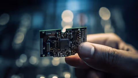
Stacking chips upward marks a shift from old layouts. Instead of spreading circuits flat across a surface, engineers now build in layers like a sandwich. Vertical arrangement saves space while boosting connections between parts. Efficiency climbs because signals travel shorter paths through stacked levels.
Stacking chips in three dimensions alters how fast computers run, showing up lately in smarter machines, phones, faster circuits. This new layout packs parts tighter, works quicker without needing more room.
Basics of 3D Chip Stacking
Stacked like pancakes, 3D chips pile circuits up instead of laying them out wide. Not spread thin but built tall, they rely on tiny vertical bridges between levels. Tiny wires punch through layers - connecting pieces without stretching sideways. This shape saves space while letting parts talk fast. Upward growth swaps sprawl for height, fitting more into less room.
Stacking chips vertically opens new paths when sideways growth hits limits. Shrinking gadgets while boosting power pushes design beyond flat arrangements.
By using vertical stacking, semiconductor designers can:
- Close gaps in how parts talk to each other
- Improve data transfer rates
- Save physical space
- Lower energy usage
- Increase transistor density
Stacking things higher feels like how cities grow once they run out of room sideways.
3D chip stacking changes how semiconductors work today
Now things shift when tiny switches can’t shrink any further. Still, pushing silicon limits brings new ideas into play.
Dealing with Physical Size Limits
Years went by while chips evolved much like shrinking transistors did. Yet tiny transistor scales bring issues along - things like:
- Heat generation
- Power leakage
- Manufacturing complexity
- Signal delay
- Increased production difficulty
Stacked layers can boost speed in fresh ways. Performance gains come through vertical designs now too.
Supporting Advanced Computing Needs
Modern technologies require large amounts of data processing:
- Artificial intelligence systems
- Cloud computing platforms
- Mobile processors
- Graphics processing
- Edge computing devices
Faster links between processors and memory help these apps run more smoothly.
Understanding 3D chip stacking
What seems tricky at first becomes clear once broken down into smaller parts.
Layer Creation
One by one, each semiconductor layer gets made on its own. Though separate, they handle distinct jobs when combined.
Examples include:
- Processing cores
- Memory modules
- Input/output systems
- Specialized accelerators
Vertical Integration
One layer sits on top of another, held in place by careful production techniques.
Through-Silicon Vias (TSVs)
Poking through silicon like tiny tunnels, Through-Silicon Vias form the backbone of 3D chip stacking. These microscopic pathways carry signals up and down between layers. Instead of spreading out sideways, circuits now climb. Hidden inside advanced chips, they behave like elevators for electricity. Their presence allows components to nest tightly together. Without them, stacking would hit a wall. Built directly into the material, these links cut distances signals must travel. Performance gains come not from speed alone but from smart placement.
TSVs create direct communication channels between chip layers.
Benefits include:
- Faster signal movement
- Reduced latency
- Better bandwidth
- Lower power consumption
3D Chip Stacking Methods
Several approaches exist within this field.
Stacked chips link straight to one another, often found in niche computing hardware. Before slicing into pieces, full wafers get piled up - typical in mass production setups. Single dies fastened onto bigger wafers show up in next-gen storage tech. Metal meets metal across levels, making powerful circuits possible through bonded fusion.
One way might work better if the project needs certain features. Another could fit when simplicity matters most.
Three dimensional chip stacking advantages
Faster Performance
Built closer together, parts on a chip exchange information faster. Distance shrinks, speed jumps. Signals hop across gaps in tiny moments. Less space to cross means quicker responses. Tiny trips add up to big time savings.
This can improve:
- Processing speed
- Memory access
- System responsiveness
Better Energy Efficiency
Far-reaching wires need extra power to keep things running. Power loss grows when electricity travels long distances.
Fewer watts are needed when chips pile up, simply because signals travel shorter paths.
This matters more when considering:
- Portable devices
- Data centers
- Embedded systems
Space Optimization
Fewer spaces inside gadgets push engineers toward tighter layouts. Tiny components now fit where older parts once filled whole boards.
Fitting extra features into tight spaces becomes possible when layers are built upward. A manufacturer might stack components like pancakes - each level adding power without spreading wide.
Examples include:
- Smartphones
- Wearable technology
- Compact computing systems
Improved Memory Integration
Stacking techniques can boost memory setups in noticeable ways.
Stacked designs let memory sit near processing units in high-speed setups. Built-up layers help move data faster by shrinking the distance chips must travel. Closer placement cuts delays when pulling information. These arrangements pack storage tight beside compute parts. Vertical builds improve flow between brain and recall sections of systems.
Benefits include:
- Faster memory communication
- Reduced bottlenecks
- Better performance in data-heavy tasks
3D chip stacking trends
Lately, more folks are turning their attention to high-end packaging methods.
Artificial Intelligence Hardware
Floods of data move through AI tasks. Yet each step handles pieces at a time.
Putting layers together can make data move faster from chip to storage. Sometimes it's about how close things sit, not just what they do.
This supports:
- Machine learning operations
- Neural network processing
- large-scale data analysis
Hybrid Bonding Advancements
Little ridges sit between sheets in old-school setups.
Built on newer methods, hybrid bonding links parts closer than before. Efficiency jumps when these bonds form through advanced steps. Tighter contact happens without extra bulk getting in the way. Progress shows most where connection quality improves silently.
Potential advantages include:
- Increased density
- Faster communication
- Lower power use
Chiplet Integration
These days, chip creators are shifting away from building a single big piece. Tiny chunks of circuitry - known as chiplets - are stepping into the spotlight. Rather than crafting one monolithic block, engineers now link compact units together. This approach swaps old methods for something more flexible. Miniaturized parts connect like puzzle pieces, forming powerful systems without needing everything on one slab.
Stacking chips in three dimensions opens new ways to build systems. Tiny chip pieces fit together like blocks, changing how designs take shape.
Folks are starting to look closely at this method when building next-gen chips.
Challenges and Key Points to Keep in Mind
Though it brings benefits, real-world issues still pop up now and then.
Heat Management
Putting one layer on top of another packs more heat into the same space.
Trapped warmth builds up when caught between sheets, slowing down how fast things cool off.
Researchers continue exploring:
- Improved cooling methods
- Better materials
- Thermal design strategies
Manufacturing Complexity
Built on tiny scales, stacking chips demands highly tuned manufacturing tricks. Layers snap together only when machinery moves without error.
Challenges include:
- Yield optimization
- Structural accuracy
- Testing procedures
Design Compatibility
Some chip uses gain more than others when layers are stacked upward.
Engineers must evaluate:
- Performance requirements
- Thermal considerations
- system architecture needs
Myths Around 3D Chip Stacking
Not everything people think about this tech is true.
Some think extra layers automatically improve results. Yet deeper networks can struggle without proper training. A single added layer might help. Other times it just slows things down. Performance depends on more than depth alone.
What you get hinges on how it is built plus what tasks must run.
Misunderstanding 2: Stacking completely replaces traditional chips.
Reality: Conventional designs remain important in many applications.
Misunderstanding 3: It only benefits large computing systems.
Smaller gadgets? They gain too. Phones, tablets - those count. Even tiny tech sees the upside. Not just big machines anymore. Little things move better now.
Conclusion
What if chips could do more by building upward? Stacking them in three dimensions lets semiconductors run faster, cooler, fewer delays. That quiet shift explains the growing interest in today's tech designs - no flash, just function.
Stacking chips upward lets engineers boost how fast they talk to each other, while also shrinking size and using less power. Even so, handling overheating issues and tricky production methods still steer where things go next.
When computers need more power, old ways of building chips hit a wall. So instead of spreading out, stacking layers up high could keep progress moving forward. This shift might just be how future chips grow smarter without growing wider.