How Tiny Transistors Continue to Shrink Modern Chips: Understanding the Future of Semiconductor Technology
Modern devices such as smartphones, laptops, gaming systems, and data centers rely on powerful computer chips. At the center of these chips are tiny components called transistors. Over many decades, engineers have continuously reduced the size of transistors to fit more computing power into smaller spaces.
Inside today’s tech boom lies shrinking transistor size on computer chips. Faster processing shows up when these pieces get tinier, yet they sip power instead of guzzling it. Tiny switches mean room for smarter tasks without bulk. Progress hides in reductions most never see.
What makes today’s gadgets so powerful yet small? The answer lies in how this tech works. It shows progress isn’t about bulkier parts but smarter design. Size shrinks while performance jumps ahead. Efficiency drives these changes behind the scenes. Tiny components now do what used to take much larger systems. This shift didn’t happen overnight. Years of refinement shaped the devices we rely on daily.
Basics of Tiny Transistors
A tiny switch on a chip handles electric pulses - each one guiding how current moves through circuits. Working in huge groups, these switches manage math tasks, handle information flow, plus carry out commands across systems.
Back then, machines filled rooms because their parts were huge. Little by little, builders figured out how to shrink transistors way down.
Transistor Shrinking Explained Simply?
Smaller transistors mean more can fit onto one chip. What once took up space now squeezes into tighter spots. Size drops, count goes up. Chips pack denser arrangements as each piece shrinks. Room opens when components get tinier. More units settle on the surface without growing the base.
Smaller transistors generally provide:
- Higher processing capability
- Reduced energy usage
- Better space efficiency
- Faster signal movement
- Improved device performance
Few concepts have steered chip progress so long. Still, its influence runs deeper than most notice.
Moore s Law and How Chips Shrink
Every now then comes talk about how tiny parts inside computers keep shrinking. One idea tied closely to this change is known as Moore's Law. Over years, chips began packing twice as many switches - give or take - on each new version. Growth like that didn’t just happen by accident.
Finding new ways isn’t easier now, yet those who design chips keep pushing with fresh ideas anyway. Despite tougher conditions, clever tweaks still emerge from labs focused on speed and size.
How Small Transistors Shape Today's Computer Chips
Few realize how tiny switches inside gadgets shape much of modern life. Tiny changes here ripple through devices everyone relies on.
Improved Performance
Inside the same space on a chip, extra transistors find room. Because of that, chips sometimes handle many computations at once.
Examples include:
- Faster application loading
- Better gaming performance
- Advanced artificial intelligence processing
- Efficient multitasking
- Enhanced graphics capability
Better Energy Efficiency
Tiny parts usually need less energy to run.
This can help:
- Extend device battery life
- Reduce heat production
- Lower energy consumption in large computing systems
- Improve overall system efficiency
Supporting Advanced Technologies
Modern developments depend on powerful semiconductor designs:
Tiny Transistors Power AI Calculations. Small Chips Enable Smartphone Performance. Transistors Scale Cloud Computing Needs. Sensors Processed by Miniature Electronics. Efficient Wearables Driven by Micro Components. Data Center Capacity Expanded Through Tiny Switches. Autonomous Systems Rely on Compact Processing Units.
Small transistors keep shrinking chips
Smaller transistors? It's more than just shrinking what we already have. Different methods pop up when new tools enter the scene. Materials shift, then performance shifts too.
Designing smaller structures
Fine lines on chips get drawn by engineers, working at sizes you cannot see. Tiny switches fit together, built piece by piece in spaces narrower than a strand of hair.
A single step across a tiny line takes you through just one billionth of a meter. That distance has its own name - nanometer.
Examples of manufacturing scales include:
- 14nm
- 10nm
- 7nm
- 5nm
- 3nm
Each step marks a new phase in how chips are made over time.
Using Lithography Technology
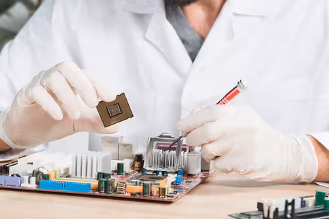
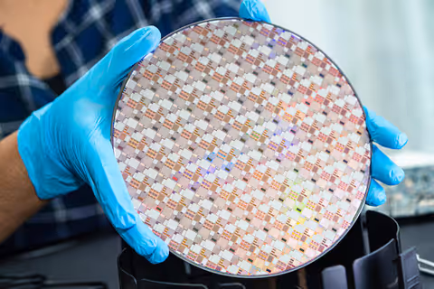
Starting with light, makers etch tiny lines on smooth silicon disks. Instead of ink, they rely on precise beams to draw each design. Patterns form when those rays pass through a stencil-like mask. What emerges is a map for how electricity will flow later. Tiny details get locked into place during development steps after exposure. Each wafer carries many chips once patterning finishes.
Laser tools shape tiny patterns with sharp accuracy inside modern machines. Built using careful methods, these setups deliver fine results through steady beams of light.
The process involves:
- Applying special materials to silicon
- Projecting circuit patterns
- Etching structures
- Building transistor layers
- Repeating multiple manufacturing steps
On one chip, you can fit billions of minuscule parts. A single piece holds countless microscopic units packed together. Tiny forms crowd each chip by the billion. Each chip carries vast numbers of small features lined up tightly. Billions of little components settle onto just one surface.
New Transistor Designs Introduced
One day, old-style transistors just couldn’t keep up anymore.
Out of reach came fresh designs instead
- Fin-shaped transistors (FinFET)
- Gate-All-Around designs
- Three-dimensional transistor structures
- Stacked architectures
Smaller builds keep working well because these layouts boost precision. When dimensions drop, function stays strong thanks to smarter structure choices.
Miniaturization Efficiency Integration Speed Materials
Several factors influence ongoing transistor development.
Advanced Materials
Even though silicon sticks around, scientists keep hunting for different options.
Examples include:
- Silicon-germanium
- High-k materials
- Compound semiconductors
- Two-dimensional materials
Performance could stay strong even when things get super tiny, thanks to these substances.
Three-Dimensional Chip Structures
Upward growth now takes priority over spreading out, as designers shift their focus skyward.
Benefits include:
- More transistor density
- Better space usage
- Shorter signal pathways
- Higher processing efficiency
Packaging Innovation
Inside today's tech, how chips are packed shapes speed gains just as much as design tweaks. A quiet force behind faster devices sits not in circuits alone but in their wrapping.
Working together smoothly happens when chip parts link through newer techniques.
new directions in small transistor advances
Recent semiconductor advancements focus on overcoming physical limitations.
Smaller Manufacturing Nodes
Fresh methods in production keep drawing attention from makers worldwide. Yet, trial runs shape how factories adapt over time. Still, changes emerge slowly across the industry landscape.
Current developments emphasize:
- 3nm architectures
- research into 2nm processes
- advanced transistor geometries
- denser chip designs
AI used to make computer chips
Few realize how often machines now guide those building tiny computing parts.
AI tools can:
- Optimize layouts
- identify design issues
- improve manufacturing efficiency
- reduce design complexity
Research Beyond Silicon
Focusing ahead, researchers keep exploring options able to assist shrinking tech even more.
Among the spots being looked at are:
- Carbon nanotubes
- Quantum materials
- Two-dimensional semiconductor layers
- Novel transistor architectures
These technologies remain active research areas.
Common Challenges and Considerations
Even tiny switches bring problems along with benefits.
Heat Management
Packed tight, tiny parts tend to trap heat. Heat builds up when little pieces sit near one another.
Heat beyond normal levels can impact:
- Reliability
- efficiency
- performance stability
Engineers must create effective cooling approaches.
Manufacturing Complexity
Fine details on small transistors demand careful crafting during manufacturing.
Challenges include:
- microscopic defects
- complex fabrication steps
- increasing engineering requirements
- precision limitations
Physical Limits
Funny thing - tiny things start acting odd when they’re too small. Electricity doesn’t follow normal rules down there.
Still, scientists work on fresh methods to tackle such gaps in knowledge.
Conclusion
These days, chips get their power by packing in ever tinier switches. Because they're smaller, computers can do more without guzzling extra energy. Devices fit easier into tight spaces since everything inside takes up less room.
Even so, tough problems keep showing up for engineers, yet fresh solutions emerge from smarter materials, inventive chip parts, instead of old methods. What happens inside tiny circuits still drives how computers work later on, also changes how people interact with devices.